“Fast growth in Internet of Things (IoT) has attracted a lot of attention of flexible and easily processable hybrid organic-inorganic nanomaterials, integrated into modern electronics and applied in multidisciplinary fields. Nanoporous and microporous thin films with regularly ordered pores exemplified by honeycomb films have received considerable interest due to its diverse potential applications, such as optoelectronics, microstructured electrodes, sensors, and charge storage devices, synthetic templates for nanoparticles, catalytic supports with large surface areas, scaffold materials in biotechnology and separation. Various materials have been applied for the synthesis of the honeycomb structures, such as star polymers, hyperbranched polymers, surfactant-encapsulated polyoxometalate for polystyrene, cross-linkable monomers,and biological molecules.”*
In the article cited here Sajjad Husain Mir and Bungo Ochiai have investigated the factors affecting the micro-structuration of the polymer-Ag honeycomb films and investigated the I-V characteristics. The pore sizes of the polymer-Ag honeycomb films were feasibly tuned by altering various parameters, namely, casting volume, polymer concentration, and molecular weight of the grafted poly(methyl methacrylate) (PMMA) chain.*
The current-sensing scanning probe microscopy (CSSPM) images for this article were taken using a NANOSENSORS™ Platinum-Silicide AFM probe. ( PtSi-CONT ).
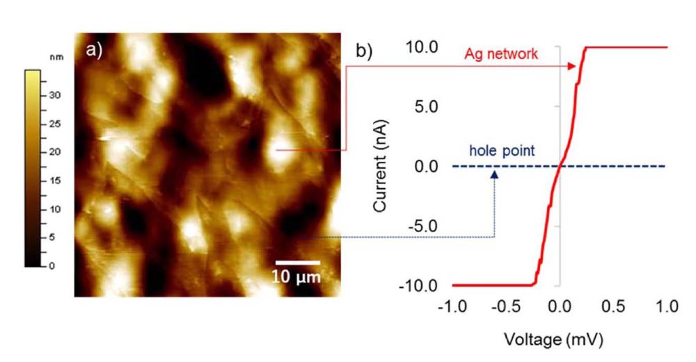
Figure 6 from Mir & Ochiai “Conductive Polymer-Ag Honeycomb Thin Film: The Factors
Affecting the Complexity of the Microstructure*
a) Topography SPM image, and b) I-V curves of the polymer-Ag honeycomb film on HOPG (preparation conditions for polymer-Ag honeycomb film: poly(NVK-co-MAH)-g-PMMA from PMMA (Mn=2100), 0.3 mg mL−1 and 50μL; measurement conditions: topography SPM image was taken by contact mode using microfabricated PtSi-coated cantilever (f0: 15 kHz, C: 0.2 N m−1), and the I-V curves were taken at specific points.
*Sajjad Husain Mir, Bungo Ochiai
Conductive Polymer-Ag Honeycomb Thin Film: The Factors Affecting the Complexity of the Microstructure
Journal of The Electrochemical Society, 165 (8) B3030-B3034 (2018)
JES Focus issue on ubiquitous sensors and systems for IOT
DOI: 10.1149/2.0031808jes
Open Access The article “Conductive Polymer-Ag Honeycomb Thin Film: The Factors Affecting the Complexity of the Microstructure” by Sajjad Husain Mir and Bungo Ochiai is licensed under a Creative Commons Attribution 4.0 International License, which permits use, sharing, adaptation, distribution and reproduction in any medium or format, as long as you give appropriate credit to the original author(s) and the source, provide a link to the Creative Commons license, and indicate if changes were made. The images or other third party material in this article are included in the article’s Creative Commons license, unless indicated otherwise in a credit line to the material. If material is not included in the article’s Creative Commons license and your intended use is not permitted by statutory regulation or exceeds the permitted use, you will need to obtain permission directly from the copyright holder. To view a copy of this license, visit https://creativecommons.org/licenses/by/4.0/.