Diamond has a high breakdown field, high carrier mobilities and the highest thermal conductivity. That is why diamond is a promising material for next generation high-power devices such as field effect transistors.*
In their paper “Conductive-probe atomic force microscopy and Kelvin-probe force microscopy characterization of OH-terminated diamond (111) surfaces with step-terrace structures”, Masatsugu Nagai, Ryo Yoshida, Tatsuki Yamada, Taira Tabakoya, Christoph E. Nebel, Satoshi Yamasaki, Toshiharu Makino, Tsubasa Matsumoto, Takao Inokuma and Norio Tokuda report about a detailed characterization of OH-terminated diamond (111) surfaces with step-terrace (ST) and bunching-step (BS) regions. In order to obtain the OH-terminated diamond (111) surfaces, they combined three techniques: anisotropic diamond etching by thermochemical reaction between Ni and diamond in high-temperature water vapor, hydrogen plasma treatment24) and water vapor annealing.
For characterization of the topography as well as electronic surface properties, atomic force microscopy (AFM), Kelvin-probe force microscopy (KPFM) and conductive-prove AFM (CPAFM) were applied.*
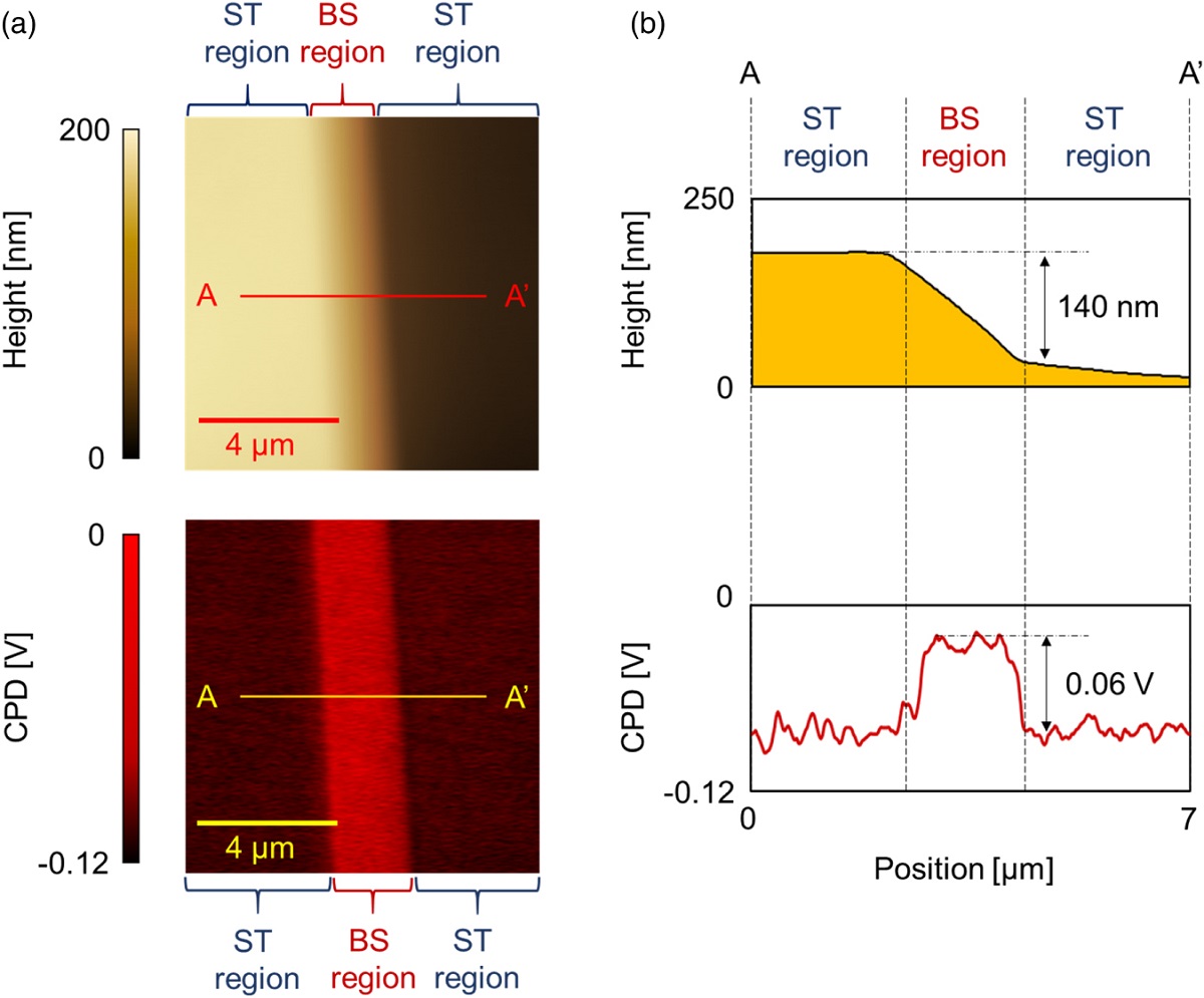
They found that the contact potential difference (CPD) and current were highly correlated with the surface topography and concluded that the interface states were generated around steps on the OH-terminated diamond (111) surfaces.*
The results presented in this paper indicate that atomically flat diamond surfaces with minimal step densities are required to form ideal MOS structures with minimized interface state densities.*
The CPD maps of the OH-terminated diamond (111) surfaces were obtained by the KPFM measurements, using NANOSENSORS™ Platinum Silicide ( PtSi ) AFM probes. *

Fig. 2 from “Conductive-probe atomic force microscopy and Kelvin-probe force microscopy characterization of OH-terminated diamond (111) surfaces with step-terrace structures” by Masatsugu Nagai et al.:
(Color online) (a) The topographic image and CPD map of the OH-terminated diamond (111) surface with ST and BS regions. (b) the cross sectional image and CPD profile corresponding to the line A-A’ in the Fig. 2(a).
*Masatsugu Nagai, Ryo Yoshida, Tatsuki Yamada, Taira Tabakoya, Christoph E. Nebel, Satoshi Yamasaki, Toshiharu Makino, Tsubasa Matsumoto, Takao Inokuma and Norio Tokuda
Conductive-probe atomic force microscopy and Kelvin-probe force microscopy characterization of OH-terminated diamond (111) surfaces with step-terrace structures
Japanese Journal of Applied Physics, 2019, Volume 58, Number SIIB08
DOI: https://doi.org/10.7567/1347-4065/ab1b5c
Please follow this external link for the full article: https://iopscience.iop.org/article/10.7567/1347-4065/ab1b5c
Open Access: The article “Conductive-probe atomic force microscopy and Kelvin-probe force microscopy characterization of OH-terminated diamond (111) surfaces with step-terrace structures” by Masatsugu Nagai, Ryo Yoshida, Tatsuki Yamada, Taira Tabakoya, Christoph E. Nebel, Satoshi Yamasaki, Toshiharu Makino, Tsubasa Matsumoto, Takao Inokuma and Norio Tokuda is licensed under a Creative Commons Attribution 4.0 International License, which permits use, sharing, adaptation, distribution and reproduction in any medium or format, as long as you give appropriate credit to the original author(s) and the source, provide a link to the Creative Commons license, and indicate if changes were made. The images or other third party material in this article are included in the article’s Creative Commons license, unless indicated otherwise in a credit line to the material. If material is not included in the article’s Creative Commons license and your intended use is not permitted by statutory regulation or exceeds the permitted use, you will need to obtain permission directly from the copyright holder. To view a copy of this license, visit http://creativecommons.org/licenses/by/4.0/