In the last years, Transition Metal Dichalcogenides (TMDs) -based p-n junctions have been extensively studied and a variety of prototypes such as light-emitting diodes, photodetectors, or photovoltaic devices have been developed. *
Recently, the possibility of using ferroelectric substrates to modulate the carrier type in TMDs has been also demonstrated enabling the formation of lateral p-n homojunctions without the need of external gating. However, while the electrical properties of these systems have been extensively studied in previous works, the optical features of p-n homojunctions have not received much attention, and there has been limited research on how TMDs photoluminescence (PL) is modulated at the interfaces of these junctions. *
The association of 2D materials and ferroelectrics offers a promising approach to tune the optoelectronic properties of atomically thin Transition Metal Dichalcogenides (TMDs). *
In the article “Light-Induced Ferroelectric Modulation of p-n Homojunctions in Monolayer MoS2” by Mariola O Ramirez, Jaime Fernandez-Tejedor, Daniel Gallego, Javier Fernández-Martinez, Pablo Molina, David Hernández-Pinilla, Julio Gómez-Herrero, Pablo Ares and Luisa E. Bausá, the combined effect of ferroelectricity and light on the optoelectronic properties of monolayer (1L)-MoS2 deposited on periodically poled lithium niobate crystals is explored. *
Using scanning micro-photoluminescence, the effect of excitation intensity, scanning direction, and domain walls on the 1L-MoS2 photoluminescence properties is analyzed, offering insights into charge modulation of MoS2. *
The findings unveil a photoinduced charging process dependent on the ferroelectric domain orientation, in which light induces charge generation and transfer at the monolayer-substrate interface. *
This highlights the substantial role of light excitation in ferroelectrically-driven electrostatic doping in MoS2. *
Additionally, the work provides insights into the effect of the strong, nanometrically confined electric fields on LiNbO3 domain wall surfaces, demonstrating precise control over charge carriers in MoS2, and enabling the creation of deterministic p-n homojunctions with exceptional precision. The results suggest prospects for novel optoelectronic and photonic application involving monolayer TMDs by combining light-matter interaction processes and the surface selectivity provided by ferroelectric domain structures. *
To corroborate the optical results, Mariola O Ramirez et al. measured current-voltage (I-V) curves by using two AFM cantilevers with platinum-coated nanometer-radius tips in contact with the 1L-MoS2 i) on a single domain region, and ii) on both sides of a ferroelectric domain wall where the p-n junction is formed. The results are shown in Figure 3c. (as cited in this blogpost). *
The electrical characterization was carried out by means of a home-built two-terminal probe station with 2 sets of xyz piezomotors that allow precise positioning of the electrical probes. *
These were NANOSENSORS™ AdvancedTEC™ ATEC-EFM tip-view AFM probes, conductive AFM tips that protrude from the very end of the AFM cantilever (with a nominal stiffness of 2.8 N m−1), ensuring real AFM tip visibility from above for a soft and accurate mechanical and electrical contact. *
To characterize the electrical properties of the system, the ATEC-EFM probes were brought into direct contact with the MoS2 flakes (see Figure 3c as cited in this blogpost), as verified using a force sensor with a sensitivity of ≈1 mN located underneath the sample. This ensures a good electrical contact between the AFM probes and the MoS2. *
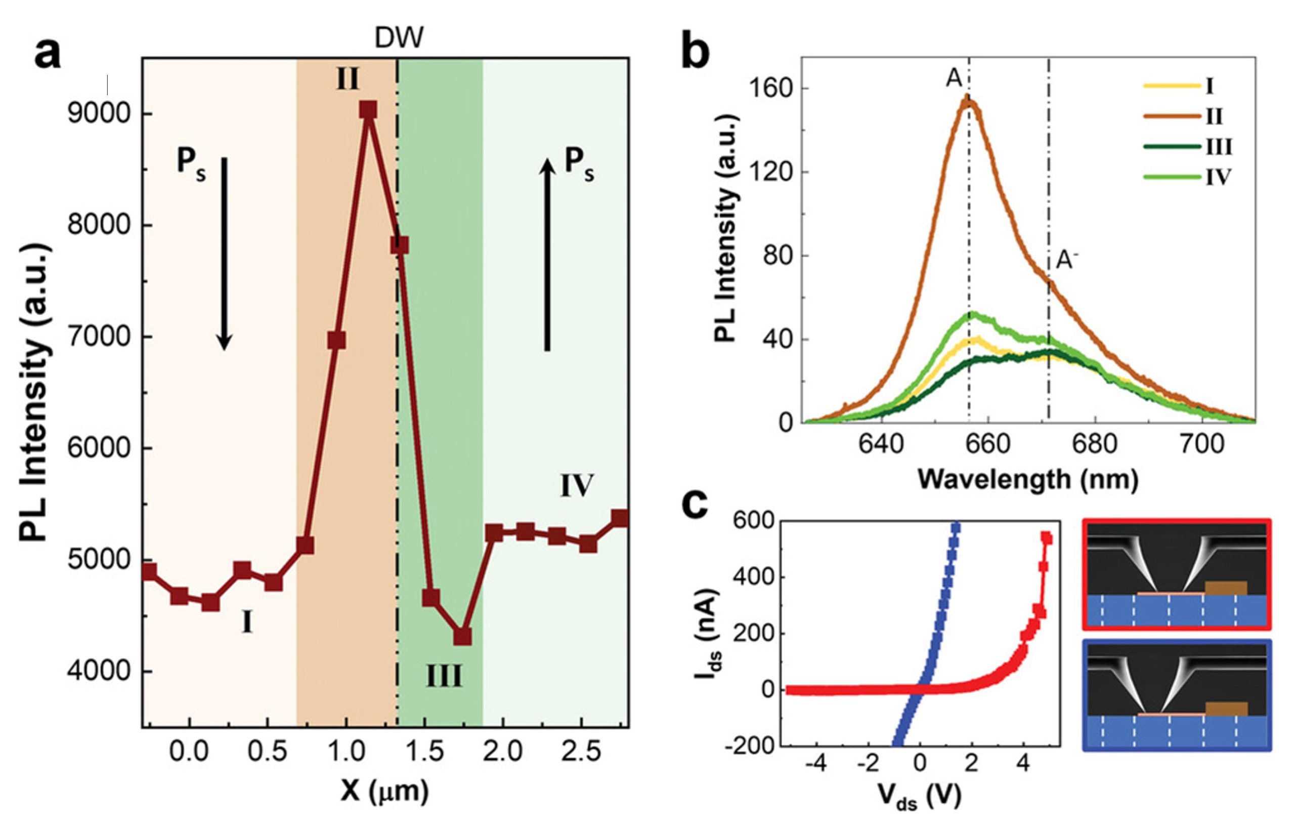
Figure 3 from Mariola O Ramirez et al. 2024 “Light-Induced Ferroelectric Modulation of p-n Homojunctions in Monolayer MoS2”:
Nanometric control over charge carriers in MoS2. a) Integrated PL intensity of 1L-MoS2 on the vicinity of a ferroelectric domain wall in LiNbO3 for an excitation intensity close to 103 W cm−2. b) PL spectra of 1L-MoS2 in different regions: I and IV correspond to the Pdown and Pup domain surfaces, respectively; II and III correspond to the vicinities of the domain wall surfaces. The spectral positions of the exciton (A) and trion (A−) bands are indicated. c) Dark intensity-voltage (I–V) curves measured contacting the 1L-MoS2 by using two Pt-coated tips on a same single domain surface (blue) and both sides of a single domain wall (red). Schematics of the experimental configuration are shown in the right panels.
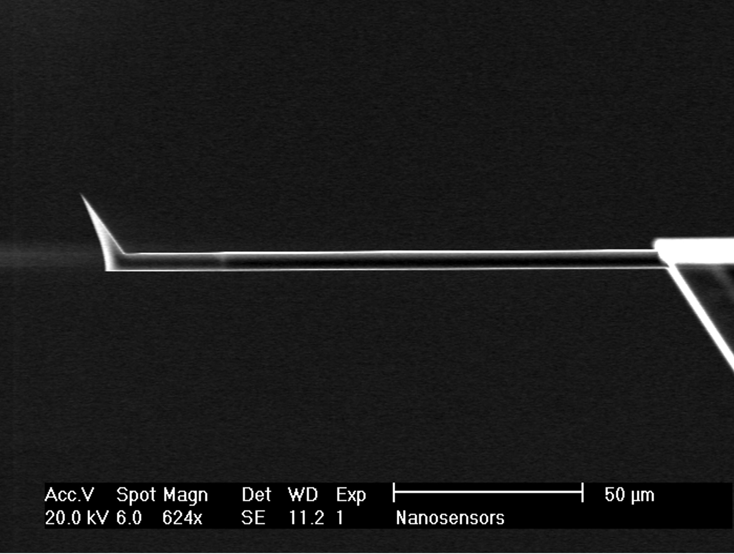
SEM image of NANOSENSORS™ AdvancedTEC™ tip-view AFM probe – side view of AFM tip and AFM cantilever
*Mariola O Ramirez, Jaime Fernandez-Tejedor, Daniel Gallego, Javier Fernández-Martinez, Pablo Molina, David Hernández-Pinilla, Julio Gómez-Herrero, Pablo Ares and Luisa E. Bausá
Light-Induced Ferroelectric Modulation of p-n Homojunctions in Monolayer MoS2
Advanced Optical Materials 2024, 12, 2400624
DOI: https://doi.org/10.1002/adom.202400624
The article “Light-Induced Ferroelectric Modulation of p-n Homojunctions in Monolayer MoS2” by Mariola O Ramirez, Jaime Fernandez-Tejedor, Daniel Gallego, Javier Fernández-Martinez, Pablo Molina, David Hernández-Pinilla, Julio Gómez-Herrero, Pablo Ares and Luisa E. Bausá is licensed under a Creative Commons Attribution 4.0 International License, which permits use, sharing, adaptation, distribution and reproduction in any medium or format, as long as you give appropriate credit to the original author(s) and the source, provide a link to the Creative Commons license, and indicate if changes were made. The images or other third-party material in this article are included in the article’s Creative Commons license, unless indicated otherwise in a credit line to the material. If material is not included in the article’s Creative Commons license and your intended use is not permitted by statutory regulation or exceeds the permitted use, you will need to obtain permission directly from the copyright holder. To view a copy of this license, visit https://creativecommons.org/licenses/by/4.0/.