Skip to content

high resolution imaging

Transparent electrodes based on molybdenum-titanium-oxide with increased water stability for use as hole-transport/hole-injection components

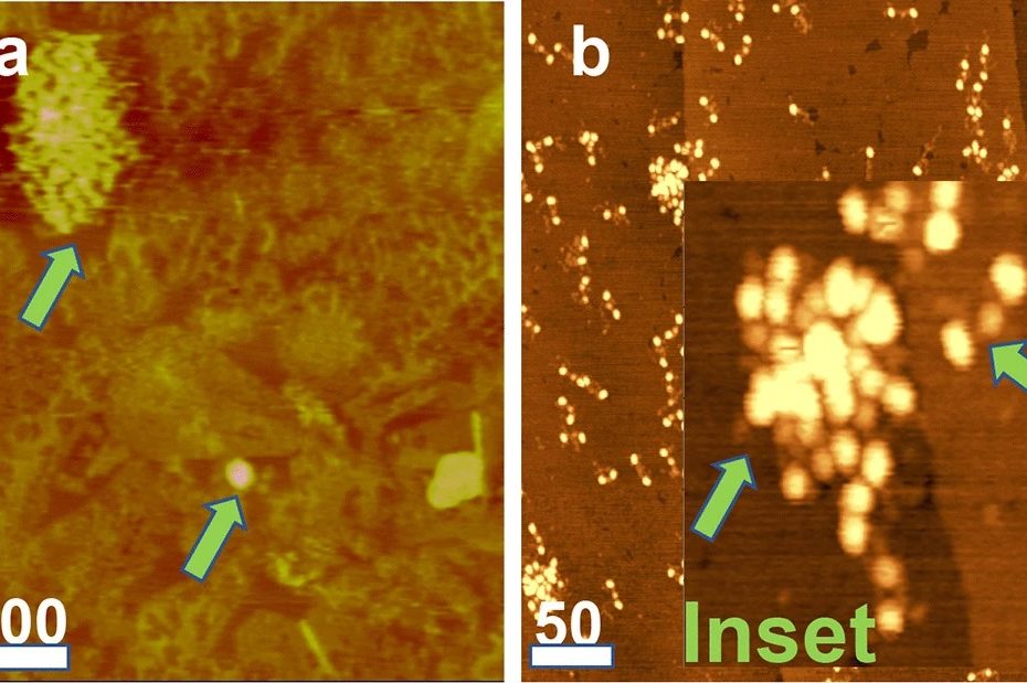
Figure 6 from Selina Goetz et al. 2022 “Transparent electrodes based on molybdenum–titanium–oxide with increased water stability for use as hole-transport/hole-injection components”: AFM images of a bare glass, b bare PET, c MTO40/Ag14/MTO10/30 on glass and d MTO40/Ag14/MTO10/30 on PET Figure 6 displays the 1 × 1 µm2 AFM images of the DMD on glass and PET, as well as the corresponding bare substrate. The roughness of the electrodes is mostly affected by the underlying substrate. The extracted root mean square value (RMS) for the glass substrate (Fig. 6a) is 1.8 ± 0.1 nm and 11.5 ± 4.0 nm for the PET substrate (Fig. 6b). The RMS values of the DMD electrodes are even reduced, yielding RMS = 1.0 ± 0.1 nm for glass/MTO40/Ag14/MTO10/30 (Fig. 6c) and RMS = 4.8 ± 2.0 nm for PET/MTO40/Ag14/MTO10/30 (Fig. 6d). NANOSENSORS silicon high-resolution AFM probes for tapping mode with a typical AFM tip radius of 2 nm ( SuperSharpSilicon™ SSS-NCHR ) were used.

The application of molybdenum oxide layers in electronic devices like solar cells and organic light emitting diodes (LEDs) has expanded considerably. * Dielectric/metal/dielectric (DMD) transparent… Read More »Transparent electrodes based on molybdenum-titanium-oxide with increased water stability for use as hole-transport/hole-injection components
Rapid access to discrete and monodisperse block co-oligomers from sugar and terpenoid toward ultrasmall periodic nanostructures

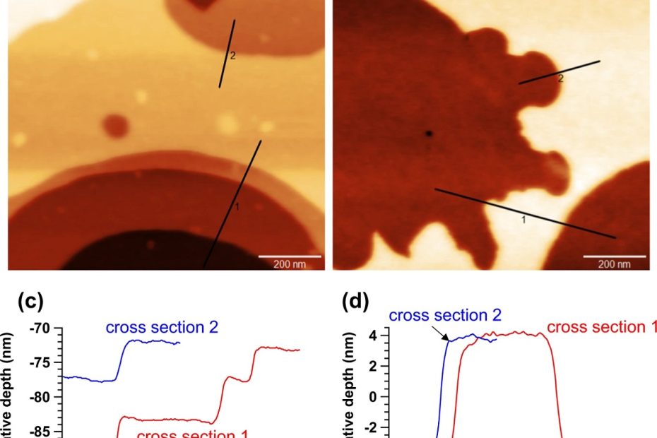
Fig. 4 from : Rapid access to discrete and monodisperse block co-oligomers from sugar and terpenoid toward ultrasmall periodic nanostructures by Takuya Isono et al. Thin-film morphologies of Glc3-b-Sol and Glc4-b-Sol. AFM height images (a, b) and corresponding cross-sectional profiles (c, d) indicating the formation of 6–8-nm-thick horizontal lamellae in Glc3-b-Sol (a, c) and Glc4-b-Sol thin films (b, d). Thin-film samples were prepared by spin-coating the BCO solution onto the hydrophilic surface of a silicon substrate followed by thermal annealing at 85 °C for 1 h. NANOSENSORS PointProbe Plus PPP-NCHR standard silicon tapping mode AFM probes and NANOSENSORS SuperSharpSilicon high resolution silicon AFM probes were used

Discrete block co-oligomers (BCOs) can form highly ordered ultrasmall nanostructures which can be used for lithographic templates. These nanotemplates are promising for the low-cost, large-scale,… Read More »Rapid access to discrete and monodisperse block co-oligomers from sugar and terpenoid toward ultrasmall periodic nanostructures

AFM probes for high resolution imaging – NANOSENSORS SuperSharpSilicon™ series video reaches 500 views mark

The NANOSENSORS screencast on SuperSharpSilicon™ AFM probes for high resolution imaging held by Dr. Oliver Krause just passed the 500 views mark. Congratulations Oliver! NANOSENSORS™… Read More »AFM probes for high resolution imaging – NANOSENSORS SuperSharpSilicon™ series video reaches 500 views mark

视频介绍 – SuperSharpSilicon原子力显微镜探针 – NANOSENSORS™

The NANOSENSORS screencast on SuperSharp Silicon AFM tips for high resolution imaging is now available in Chinese on youtube  and youku http://v.youku.com/v_show/id_XOTIzNjg0NDQ0.html . NANOSENSORS公司的吴烨娴博士在本视频中介绍了SuperSharpSilicon原子力显微镜探针。SSS超尖硅针尖是为超高精度的原子力显微 镜成像设计的。它适用于超精细结构,如小于10nm特征粗糙度表面的测量。该探针基于NANOSENSORS的标准AFM探针 PointProbePlus系统。在一个特殊的尖端锐化过程后,针尖半径由7nm减小为2nm。… Read More »视频介绍 – SuperSharpSilicon原子力显微镜探针 – NANOSENSORS™