Happy #NanotechnologyDay!
The date, 10/9, is a nod to the nanometer scale, where objects span only billionths of a meter (10⁻⁹ meters).
We celebrate it with the nanotechnology community by featuring an article on AFM-Based Electrochemical Etching in today’s blogpost.
Nanomanufacturing involves scaled-up, reliable, and cost-effective manufacturing of nanoscale materials, structures, devices, and systems. It leads to the production of improved materials and new products, and manufactured structures with unique properties in the nanoscale are capable of enabling quantum leaps and improvement in high-performance technologies, from new sensors, high-density data storage, and drug delivery to high-strength materials and energy-efficient solar cells. These applications lead to significant demand in the future research and development of nanomanufacturing. Based on material properties, nanomanufacturing can be performed by additive, subtractive, and mass conservation. Several nanomanufacturing technologies, such as laser ablation, etching, ultraviolet light lithography, and focused ion beam (FIB), have been widely utilized to obtain functional structures and surfaces with nanoscale features. Although exciting results have been achieved, many challenges are still encountered in nanomanufacturing relative to the nanoscale, nano accuracy, complex shape/structure, and novel materials. *
Scanning probe microscopy (SPM)-based lithography, as a promising nanolithography approach for the fabrication at the nanometer scale, has attracted significant attention because of its simplicity and precise control of a structure and location. *
Atomic force microscopy (AFM), as a kind of SPM, shows more advantages in nanomanufacturing than STM, especially because AFM can work in ambient environments. Moreover, many different approaches, such as chemical and electrical methods, can be easily combined on AFM to improve the nanomanufacturing ability. AFM-based electrochemical machining was first used to modify hydrogen-passivated n-Si(111) surfaces via chemical oxidization in ambient conditions. Accordingly, the kinetics and mechanism of oxidation have attracted great interest due to the major contributions in the machining process, and other papers have hoped to improve the reproducibility of the process by studying the dynamic force microscopy modes. The comprehensive understanding and control of the oxidation mechanism are of critical importance for the application of the SPM technique. However, the complexity of challenges remains open, and the oxidation process of the sample is still complicated. Furthermore, atomic and close-to-atomic scale manufacturing (ACSM) has become the leading trend in global manufacturing development. To achieve ACSM, AFM and STM work as vital instruments due to the atomic and close-to-atomic scale resolution in all three spatial dimensions. For decades, scientists have been inspired to develop relevant techniques to ACSM to directly visualize and manipulate an individual atom using SPM. *
In their article “Toward Single-Atomic-Layer Lithography on Highly Oriented Pyrolytic Graphite Surfaces Using AFM-Based Electrochemical Etching “ Wei Han, Paven Thomas Mathew, Srikanth Kolagatla, Brian J. Rodriguez and Fengzhou Fang describe how, an AFM-based electrochemical machining method was used to etch a highly oriented pyrolytic graphite (HOPG) surface to single-atomic-layer precision.*
Atomic force microscopy (AFM)-based electrochemical etching of a highly oriented pyrolytic graphite (HOPG) surface is studied toward the single-atomic-layer lithography of intricate patterns. Electrochemical etching is performed in the water meniscus formed between the AFM tip apex and HOPG surface due to a capillary effect under controlled high relative humidity (~ 75%) at otherwise ambient conditions. The conditions to etch nano-holes, nano-lines, and other intricate patterns are investigated. The electrochemical reactions of HOPG etching should not generate debris due to the conversion of graphite to gaseous CO and CO2 based on etching reactions. However, debris is observed on the etched HOPG surface, and incomplete gasification of carbon occurs during the etching process, resulting in the generation of solid intermediates. Moreover, the applied potential is of critical importance for precise etching, and the precision is also significantly influenced by the AFM tip wear. This study shows that the AFM-based electrochemical etching has the potential to remove the material in a single-atomic-layer precision. This result is likely because the etching process is based on anodic dissolution, resulting in the material removal atom by atom.*
The experiments were performed under ambient conditions with a commercial atomic force microscope using NANOSENSORS PtIr5 coated PointProbePlus® PPP-EFM AFM probes. The AFM tip side coating enhances the conductivity of the AFM tip and allows electrical contacts, and the opposite side coating enhances the laser reflex.
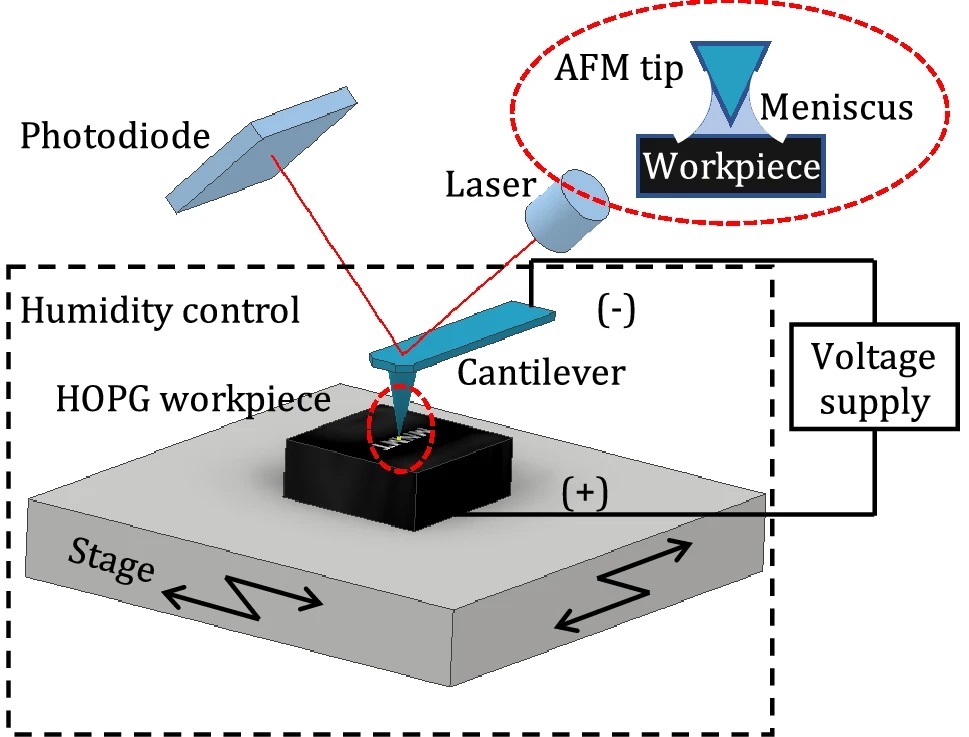
Figure 2 from Wei Han et al. “Toward Single-Atomic-Layer Lithography on Highly Oriented Pyrolytic Graphite Surfaces Using AFM-Based Electrochemical Etching”
Schematic diagram of the AFM-based electrochemical etching apparatus with an RH-controlled environment
*Wei Han, Paven Thomas Mathew, Srikanth Kolagatla, Brian J. Rodriguez AND Fengzhou Fang
Toward Single-Atomic-Layer Lithography on Highly Oriented Pyrolytic Graphite Surfaces Using AFM-Based Electrochemical Etching
Nanomanufacturing and Metrology volume 5, pages 32–38 (2022)
DOI: https://doi.org/10.1007/s41871-022-00127-9
Please follow this external link to read the full article: https://rdcu.be/cXcCi
Open Access: The article “Toward Single-Atomic-Layer Lithography on Highly Oriented Pyrolytic Graphite Surfaces Using AFM-Based Electrochemical Etching” by Wei Han, Paven Thomas Mathew, Srikanth Kolagatla, Brian J. Rodriguez and Fengzhou Fang is licensed under a Creative Commons Attribution 4.0 International License, which permits use, sharing, adaptation, distribution and reproduction in any medium or format, as long as you give appropriate credit to the original author(s) and the source, provide a link to the Creative Commons license, and indicate if changes were made. The images or other third party material in this article are included in the article’s Creative Commons licence, unless indicated otherwise in a credit line to the material. If material is not included in the article’s Creative Commons licence and your intended use is not permitted by statutory regulation or exceeds the permitted use, you will need to obtain permission directly from the copyright holder. To view a copy of this licence, visit http://creativecommons.org/licenses/by/4.0/.