Dissertation:
Rebecca Saive
Investigation of the Potential Distribution within Organic Solar Cells by Scanning Kelvin Probe Microscopy
Heidelberg 2014
http://archiv.ub.uni-heidelberg.de/volltextserver/16260/1/Dissertation_RebeccaSaive.pdf
Zhi Zhou, Haixiong Tang Henry A. Sodano
Vertically Aligned Arrays of BaTiO3 Nanowires
ACS Appl. Mater. Interfaces, 2013, 5 (22), pp 11894–11899
DOI: 10.1021/am403587q
https://pubs.acs.org/doi/abs/10.1021/am403587q
Masaharu Hirose, Eika Tsunemi, Kei Kobayashi and Hirofumi Yamada
Visualization of Charge Injection Processes in Polydiacetylene Thin Film Grains by Dual-Probe Atomic Force Microscopy
Japanese Journal of Applied Physics, Volume 52, Number 8R
DOI: https://doi.org/10.7567/JJAP.52.085201
http://iopscience.iop.org/article/10.7567/JJAP.52.085201/meta
Ian M. Craig, Matthew S. Taubman, A. Scott Lea, Mark C. Phillips, Erik E. Josberger, and Markus B. Raschke
Infrared near-field spectroscopy of trace explosives using an external cavity quantum cascade laser
Optics Express Vol. 21, Issue 25, pp. 30401-30414 (2013)
doi: https://doi.org/10.1364/OE.21.030401
https://www.osapublishing.org/oe/fulltext.cfm?uri=oe-21-25-30401&id=275124 open access
Eika Tsunemi, Kei Kobayashi, Kazumi Matsushige, Hirofumi Yamada
Development of dual-probe atomic force microscopy system using optical beam deflection sensors with obliquely incident laser beams
Review of Scientific Instruments 82, 033708 (2011)
doi: https://doi.org/10.1063/1.3534830
https://repository.kulib.kyoto-u.ac.jp/dspace/bitstream/2433/160661/1/1.3534830.pdf
Eika Tsunemi, Kei Kobayashi, Kazumi Matsushige, Hirofumi Yamada
Visualization of anisotropic conductance in polydiacetylene crystal by dual-probe frequency-modulation atomic force microscopy/Kelvin-probe force microscopy
Journal of Vacuum Science & Technology B 28, C4D24 (2010)
doi: https://doi.org/10.1116/1.3367983
https://avs.scitation.org/doi/abs/10.1116/1.3367983
Andrew C. Jones, Robert L. Olmon, Sara E. Skrabalak, Benjamin J. Wiley, Younan N. Xia, Markus B. Raschke
Mid-IR Plasmonics: Near-Field Imaging of Coherent Plasmon Modes of Silver Nanowires
Nano Lett., 2009, 9 (7), pp 2553–2558
DOI: 10.1021/nl900638p
https://pubs.acs.org/doi/abs/10.1021/nl900638p
http://nano-optics.colorado.edu/fileadmin/Publications/2009/jos_nl09.pdf


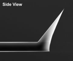
 Due to their unique geometry the tips of the AdvancedTEC probes are more susceptible to tip damage by electrostatic discharge (ESD) than other Silicon-SPM-Probes.


