Ignaas S. M. Jimidar, Kaspars Mālnieks, Kai Sotthewes, Peter C. Sherrell and Andris Šutka
Granular Interfaces in TENGs: The Role of Close-Packed Polymer Bead Monolayers for Energy Harvesters
small, Early View, Online Version of Record before inclusion in an issue, 2410155
DOI: https://doi.org/10.1002/smll.202410155
Paul P. Debes, Melanie Pagel, Simeon Muntean, Janis Hessling, Bernd M. Smarsly, Monika Schönhoff and Teresa Gatti
Functional Nanocarbon Hybrids in Metal Oxide Nanocomposites for Photocatalysis
Photochem 2025, 5(1)
DOI: https://doi.org/10.3390/photochem5010001
Petric Marc Ruya, Yan Zhao, Samuel Eyley, Wim Thielemans, Alexander Volodine, I Gede Wenten, and Xing Yang
Harnessing ion resource recovery: Design of selective cation exchange membranes via a synergistic ionic control method
Journal of Membrane Science, Volume 704, June 2024, 122844
DOI: https://doi.org/10.1016/j.memsci.2024.122844
Qian Zhang, Yulong Wang, Cameron Nickle, Ziyu Zhang, Andrea Leoncini, Dong-Chen Qi, Kai Sotthewes, Alessandro Borrini, Harold J. W. Zandvliet, Enrique del Barco, Damien Thompson and Christian A. Nijhuis
Molecular switching by proton-coupled electron transport drives giant negative differential resistance
Nature Communications volume 15, Article number: 8300 (2024)
DOI: https://doi.org/10.1038/s41467-024-52496-y
Jorge Torrero, Tobias Morawietz, Daniel García Sanchez, Dmitry Galyamin, Maria Retuerto, Vlad Martin-Diaconescu, Sergio Rojas, José Antonio Alonso, Aldo Saul Gago, Kaspar and Andreas Friedrich
High Performance and Durable Anode with 10-Fold Reduction of Iridium Loading for Proton Exchange Membrane Water Electrolysis
Advanced Energy Materials, Volume 13, Issue 23, June 16, 2023, 2204169
DOI: https://doi.org/10.1002/aenm.202204169
Dmitry V. Bagrov, Grigory S. Glukhov, Andrey V. Moiseenko, Maria G. Karlova, Daniil S. Litvinov, Petr А. Zaitsev, Liubov I. Kozlovskaya, Anna A. Shishova, Anastasia A. Kovpak, Yury Y. Ivin, Anastasia N. Piniaeva, Alexey S. Oksanich, Viktor P. Volok, Dmitry I. Osolodkin, Aydar A. Ishmukhametov, Alexey M. Egorov, Konstantin V. Shaitan, Mikhail P. Kirpichnikov, Olga S. Sokolova
Structural characterization of β-propiolactone inactivated severe acute respiratory syndrome coronavirus 2 (SARS-CoV-2) particles
Microscopy Research & Technique, Volume 85, Issue 2, February 2022, Pages 562-569
DOI: https://doi.org/10.1002/jemt.23931
P. Bampoulis
Temperature induced dynamics of water confined between graphene and MoS2 The Journal of Chemical Physics 154, 134705 (2021)
DOI:
https://doi.org/10.1063/5.0044123
Ignaas S.M. Jimidar, KaiS otthewes, Han Gardeniers, Gert Desmet
A detailed study of the interaction between levitated microspheres and the target electrode in a strong electric field
Powder Technology, Volume 383, May 2021, Pages 292-301
DOI: https://doi.org/10.1016/j.powtec.2021.01.036
Josué J. López, Antonio Ambrosio, Siyuan Dai, Chuong Huynh, David C. Bell, Xiao Lin, Nicholas Rivera, Shengxi Huang, Qiong Ma, Soeren Eyhusen, Ido E. Kaminer, Kenji Watanabe, Takashi Taniguchi, Jing Kong, Dimitri N. Basov, Pablo Jarillo-Herrero, Marin Soljačić
Large Photothermal Effect in Sub-40 nm h-BN Nanostructures Patterned Via High-Resolution Ion Beam
Nano Micro Small, Volume 14, Issue 22, May 29, 2018, 1800072
DOI: https://doi.org/10.1002/smll.201800072
Bernhard M.Berger, Reinhard Stadlmayr, Dominic Blöch, Elisabeth Gruber, Kazuyoshi Sugiyama, Thomas Schwarz-Selinger, Friedrich Aumayr
Erosion of Fe-W model system under normal and oblige D ion irradiation
Nuclear Materials and Energy, Volume 12, August 2017, Pages 468-471
DOI: https://doi.org/10.1016/j.nme.2017.03.030
Wojciech Kwieciñski, Kai Sotthewes, Bene Poelsema, Harold J.W.Zandvliet, Pantelis Bampoulis
Chemical vapor deposition growth of bilayer graphene in between molybdenum disulfide sheets
Journal of Colloid and Interface Science, Volume 505, 1 November 2017, Pages 776-782
DOI: https://doi.org/10.1016/j.jcis.2017.06.076
https://arxiv.org/pdf/1710.01061.pdf
Pantelis Bampoulis, Vincent J. Teernstra, Detlef Lohse, Harold J. W. Zandvliet, and Bene Poelsema
Hydrophobic Ice Confined between Graphene and MoS2
The Journal of Physical Chemistry C 2016, 120, 47, 27079–27084
DOI: https://doi.org/10.1021/acs.jpcc.6b09812
https://arxiv.org/pdf/1706.00675.pdf
Luka M. Devenica, Clay Contee, Raysa Cabrejo, and Matthew Kurek
Biophysical measurements of cells, microtubules, and DNA with an atomic force microscope
American Journal of Physics 84, 301 (2016)
DOI: https://doi.org/10.1119/1.4941048
https://arxiv.org/ftp/arxiv/papers/1512/1512.05662.pdf
Edwin Dollekamp, Pantelis Bampoulis, Bene Poelsema, Harold J. W. Zandvliet, and E. Stefan Kooij
Electrochemically Induced Nanobubbles between Graphene and Mica
Langmuir 2016, 32, 26, 6582–6590
DOI: https://doi.org/10.1021/acs.langmuir.6b00777


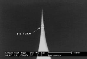
 Due to their unique geometry the tips of the are more susceptible to tip damage by electrostatic discharge (ESD) than other Silicon-SPM-Probes.
