Yutaro Katsuyama, Shunske Kayukawa, Tomoharu Tokunaga, Shunsuke Kobayashi, Shigekazu Hidaka, Atsutomo Nakamura and Takahisa Yamamoto
Variation of (001) surface structures of strontium titanate single crystals caused by flash event under direct/alternative current electric fields
Ceramics International, Volume 50, Issue 19, Part C, 1 October 2024, Pages 37366-37372
DOI: https://doi.org/10.1016/j.ceramint.2024.05.055
Yutaro Katsuyama, Ayu Kodaira, Tomoharu Tokunaga and Takahisa Yamamoto
Scanning electron microscopy observation in wide field of view for SrO/TiO2-terminated step-terrace structure formed on SrTiO3(001) single crystal surface
Journal of the Ceramic Society (2023) volume 131, issue 5, p. 135-139
DOI: https://doi.org/10.2109/jcersj2.23011
Devendra Pareek, Marco A. Gonzalez, Nedal Grewo, Marten L. Janßen, Kumarahgiri Arunakiri, Kayode Luqman Alimi, Martin Silies, Jürgen Parisi, Levent Gütay and Sascha Schäfer
Large-Area Growth of MoS2/WS2 Heterostructures by a Sequential Atomic Layer Deposition and Spin-Coating Approach
Advanced Materials Interfaces, Volume 9, Issue 31, November 3, 2022, 2200816
DOI: https://doi.org/10.1002/admi.202200816
Gaoliang Dai, Xiukun Hu, Julian Hering, Matthias Eifler, Jörg Seewig and Georg von Freymann
Define and measure the dimensional accuracy of two-photon laser lithography based on its instrument transfer function
Journal of Physics: Photonics, 2021, Volume 3, Number 3 034002
DOI: https://doi.org/10.1088/2515-7647/abfaa7
Martyn Sozanskyi, Vitalii Stadnik, Pavlo Shapoval, Iosyp Yatchyshyn, Ruslana Guminilovych, Stepan Shapoval
Optimization of Synthesis Conditions of Mercury Selenide Thin Films
Chemistry & Chemical Technology, 2020, Vo. 14, No 3, pp. 290 – 296
DOI: https://doi.org/10.23939/chcht14.03.290
Davood Momeni Pakdehi, Philip Schädlich, Thi Thuy Nhung Nguyen, Alexei A. Zakharov, Stefan Wundrack, Emad Najafidehaghani, Florian Speck, Klaus Pierz, Thomas Seyller, Christoph Tegenkamp, Hans Werner Schumacher
Silicon Carbide Stacking-Order-Induced Doping Variation in Epitaxial Graphene
Advanced Functional Materials, Volume 30, Issue 45, November 4, 2020, 2004695
DOI: https://doi.org/10.1002/adfm.202004695
Elżbieta U. Stolarczyk, Katarzyna Sidoryk, Marcin Cybulski, Marek Kubiszewski and Krzysztof Stolarczyk
Design of Therapeutic Self-Assembled Monolayers of Thiolated Abiraterone
Nanomaterials 2018, 8(12), 1018
DOI: https://doi.org/10.3390/nano8121018
J Jakubowicz, G Adamek and M Sopata
Characterization of High-Energy Ball-Milled and Hot-Pressed Nanocrystalline Tantalum
IOP Conference Series: Materials Science and Engineering, Volume 216, The 2nd International Conference on Civil Engineering and Materials Science 26–28 May 2017, Seoul, Korea
DOI: https://doi.org/10.1088/1757-899X/216/1/012006
J Jakubowcz, G Adamek, M Sopata, J K Kope and P Siwak
Hot pressing of nanocrystalline tantalum using high frequency induction heating and pulse plasma sintering
IOP Conference Series: Materials Science and Engineering, Volume 283, 6th Global Conference on Materials Science and Engineering 24–27 October 2017, Beijing, China, 283 012001
DOI: https://doi.org/10.1088/1757-899X/283/1/012001
TaskinTuna, Martin Wein, Michael Swain, Jens Fischer, Wael Att
Influence of ultraviolet photofunctionalization on the surface characteristics of zirconia-based dental implant materials
Dental Materials, Volume 31, Issue 2, February 2015, Pages e14-e24
DOI: https://doi.org/10.1016/j.dental.2014.10.008
D. Bergmann, B. Bodermann, H. Bosse, E. Buhr, G. Dai, R. Dixson, W. Häßler-Grohne, K. Hahm, and M. Wurm
Photomask linewidth comparison by PTB and NIST
Proceedings Volume 9636, Scanning Microscopies 2015; 96360S (2015) (2 November 2015); Event: SPIE Scanning Microscopies, 2015, Monterey, California, United States
DOI: https://doi.org/10.1117/12.2199453
Katharina J. Jetzschmann, Gyula Jágerszki, Decha Dechtrirat, Aysu Yarman, Nenad Gajovic-Eichelmann, Hans-Detlev Gilsing, Burkhard Schulz, Róbert E. Gyurcsányi and Frieder W. Scheller
Vectorially Imprinted Hybrid Nanofilm for Acetylcholinesterase Recognition
Advanced Functional Materials, Volume 25, Issue 32, August 26, 2015, Pages 5178-5183
DOI: https://doi.org/10.1002/adfm.201501900


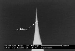
 Due to their unique geometry the tips of the are more susceptible to tip damage by electrostatic discharge (ESD) than other Silicon-SPM-Probes.
